
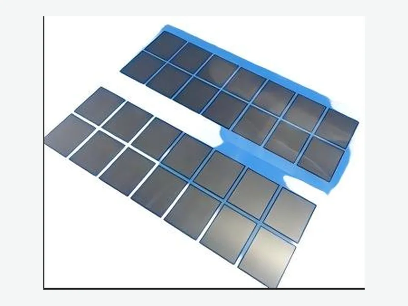
A drone ESC thermal pad must fill a variable gap without overloading the PCB or connectors. Specify deflection force at the expected bond-line thickness using the pad's force-deflection curve, then check that the resulting pressure stays below the assembly's mechanical limits.
Why Deflection Force Matters More Than Hardness
Thermal pad hardness (Shore 00) is a common shortcut, but it does not directly tell you the force the pad will exert on the PCB. Two pads with the same hardness can have different force-deflection curves because of filler loading, polymer crosslink density, and thickness. For a drone ESC, the pad sits between the MOSFETs and a heat sink or housing, and the mounting screws or clips define the compressed thickness. The force at that thickness is what bends the PCB and stresses solder joints.
A pad that is too stiff can lift the PCB locally, crack ceramic capacitors, or cause intermittent connector contact. A pad that is too soft may not develop enough contact pressure to wet the interface and achieve the expected thermal resistance. The specification must therefore be a force or pressure at a defined compression, not a durometer number alone.
- Hardness is a screening property, not a design load.
- Force-deflection curves are grade-specific and thickness-dependent.
- The installed force is set by the compressed thickness, not the free thickness.
Reading a Force-Deflection Curve for a Gap Pad
A force-deflection curve plots compressive stress (or force per unit area) against percent compression or absolute deflection. For a typical silicone gap pad, the curve is nonlinear: initial compression requires low stress, then stress rises steeply as the pad densifies. For example, a pad compressed 10% might exert 5–15 kPa, while 30% compression could require 30–80 kPa, depending on the grade. These are representative screening ranges; the exact curve must come from the selected material's data sheet.[1]
To use the curve, first determine the nominal gap and tolerance stack. The installed thickness is the gap minus any standoff or boss height. The percent compression is (free thickness - installed thickness) / free thickness. Then read the corresponding stress from the curve. Multiply by the pad area to get total force. This force is what the PCB and fasteners must react.
- Compression is calculated from free thickness and installed gap.
- Stress is read from the curve at that compression.
- Total force = stress × pad area.
Setting a Deflection Force Limit for the Drone ESC
Start with the mechanical limits of the assembly. A typical drone ESC PCB is 1.0–1.6 mm thick FR-4, often with small surface-mount components near the MOSFETs. Excessive pad force can cause visible board bow or micro-cracks in solder joints. As a screening rule, keep the pad-induced pressure below 50 kPa on the PCB area unless the board is locally supported or the design has been validated. This is a conservative starting point, not a universal limit.
Connectors and mounting hardware also impose limits. A board-to-board connector may tolerate only a few newtons of normal force before contact resistance increases or the housing deforms. If the pad sits near a connector, calculate the pad force and compare it to the connector's specified normal force limit. In many drone ESCs, the heat sink is attached with screws that pass through the PCB; the screw preload must be added to the pad force when checking board stress.
- Check PCB bow and solder joint stress, not just pad compression.
- Include connector normal force limits in the pad force budget.
- Add screw preload to pad force when evaluating total board load.
Selecting a Low-Compression-Force Pad
If the calculated force is too high, look for a pad with a lower modulus or a lower filler loading. Some silicone pads are formulated specifically for low compression force on sensitive components. For example, certain gap pads maintain thermal conductivity around 6 W/m·K while keeping compression force low enough for fragile packages. The trade-off is often a slightly higher thermal resistance at the same thickness, so the thermal budget must be rechecked.[2]
Thinner pads generally require higher stress to achieve the same percent compression because the strain gradient is steeper. If the gap allows, a thicker pad can reduce the force at a given absolute deflection. However, thicker pads add thermal resistance, so the decision is a coupled thermal-mechanical optimization.
- Low-force pads exist but may trade thermal conductivity.
- Thicker pads reduce force for the same absolute deflection.
- Always recheck thermal resistance after changing pad thickness or grade.
Validation Protocol for Drone ESC Thermal Pad Force
Before releasing the design, validate the pad force in a representative assembly. Build a fixture that mimics the actual gap, mounting method, and PCB thickness. Use a force gauge or load cell to measure the force required to compress the pad to the target thickness. Compare this to the calculated value from the data sheet curve. If the measured force is higher than expected, check for pad over-compression, misalignment, or adhesive stack effects.
Then assemble a prototype ESC and measure PCB deflection with a dial indicator or laser profilometer. Apply the pad and heat sink, and check for visible bow or component stress. Run thermal cycling (e.g., -20°C to +85°C for 100 cycles) and re-measure pad thickness and force to assess compression set. A pad with high compression set will lose contact pressure over time, increasing thermal resistance.[3]
- Measure force at target thickness with a load cell.
- Check PCB deflection in the actual assembly.
- Run thermal cycling and re-measure force to evaluate compression set.
Drawing and RFQ Inputs for a Converted Thermal Pad
When requesting a custom die-cut thermal pad, provide the nominal gap, tolerance stack, pad footprint, and target compression. Specify the maximum allowable force or pressure on the PCB. Include the operating temperature range and any electrical isolation requirement. If the pad needs adhesive on one side, state the adhesion target and the surface finish of the heat sink or PCB.[1]
FLEXCEND can review the force-deflection data for candidate grades and help select a pad that meets both thermal and mechanical limits. The final specification must be confirmed with the exact grade, thickness, adhesive stack, and test method.[1]
- Nominal gap and tolerance stack
- Pad footprint and target compression
- Maximum allowable force or pressure
- Operating temperature and electrical isolation
- Adhesive and surface finish requirements
What to send for a useful review
- Nominal gap and tolerance stack between PCB and heat sink
- Pad footprint and thickness options
- Target compression percentage or installed thickness
- Maximum allowable force or pressure on the PCB
- Connector normal force limits near the pad
- Screw preload and mounting method
- Operating and peak temperature range
- Electrical isolation requirement (if any)
- Adhesive requirement and surface finish
- Prototype quantity and annual volume
Questions teams ask during selection
How do I convert a thermal pad's force-deflection curve to a total force on the PCB?
Multiply the compressive stress (kPa) at the target compression by the pad area (m²). The result is the total force in newtons. Ensure the stress value corresponds to the exact pad thickness and grade.
What is a safe compression percentage for a drone ESC thermal pad?
Most silicone gap pads are designed for 10–30% compression. Below 10% may not ensure good contact; above 30% risks excessive force and compression set. The exact range depends on the grade and the assembly's mechanical limits.[3]
Can I use a thicker pad to reduce deflection force?
Yes, for the same absolute deflection, a thicker pad has a lower strain and therefore lower stress. However, thermal resistance increases with thickness, so the thermal budget must be re-evaluated.
How does compression set affect long-term deflection force?
Compression set is the permanent deformation after load is removed. A pad with high compression set will lose thickness and contact pressure over time, increasing thermal resistance. Select a grade with low compression set for high-temperature or long-life applications.[3]
Should I specify deflection force or pressure on the drawing?
Specify both the target compression (or installed thickness) and the maximum allowable force or pressure. This gives the converter and manufacturer a clear mechanical limit while allowing flexibility in material selection.
Sources and technical references
References support the published context and cited data. Final material and assembly decisions still require grade-specific documentation and application validation.
- Thermal Silicone Pads engineering data and screening boundariesFLEXCEND Engineering · Accessed
- Modus Advanced Inc. | Chomerics THERM-A-GAP Materials for Data Center Thermal Managementmodusadvanced.com · Accessed
- What Is a Thermal Gap Pad? - Sheen Technologysheenthermal.com · Accessed